









Executive Overview
For decades, the bleeding edge of modern optics has been defined by a paradox: while the fundamental applications of ultrafast lasers—ranging from laser-assisted eye surgery to the precise manufacturing of microprocessors—have grown increasingly ubiquitous, the instruments themselves have remained stubbornly tethered to the laboratory. Traditionally, these high-powered devices are housed in bulky, complex configurations that occupy entire optical tables, demanding stringent environmental controls, meticulous alignment, and substantial financial investment.
That paradigm is now on the verge of a fundamental disruption. A team of researchers led by Professor Tobias J. Kippenberg at the École Polytechnique Fédérale de Lausanne (EPFL), in collaboration with scientists from the Helmholtz-Zentrum Dresden-Rossendorf (HZDR), has successfully engineered the world’s first integrated ultrafast laser capable of matching the raw performance metrics of traditional tabletop femtosecond systems.
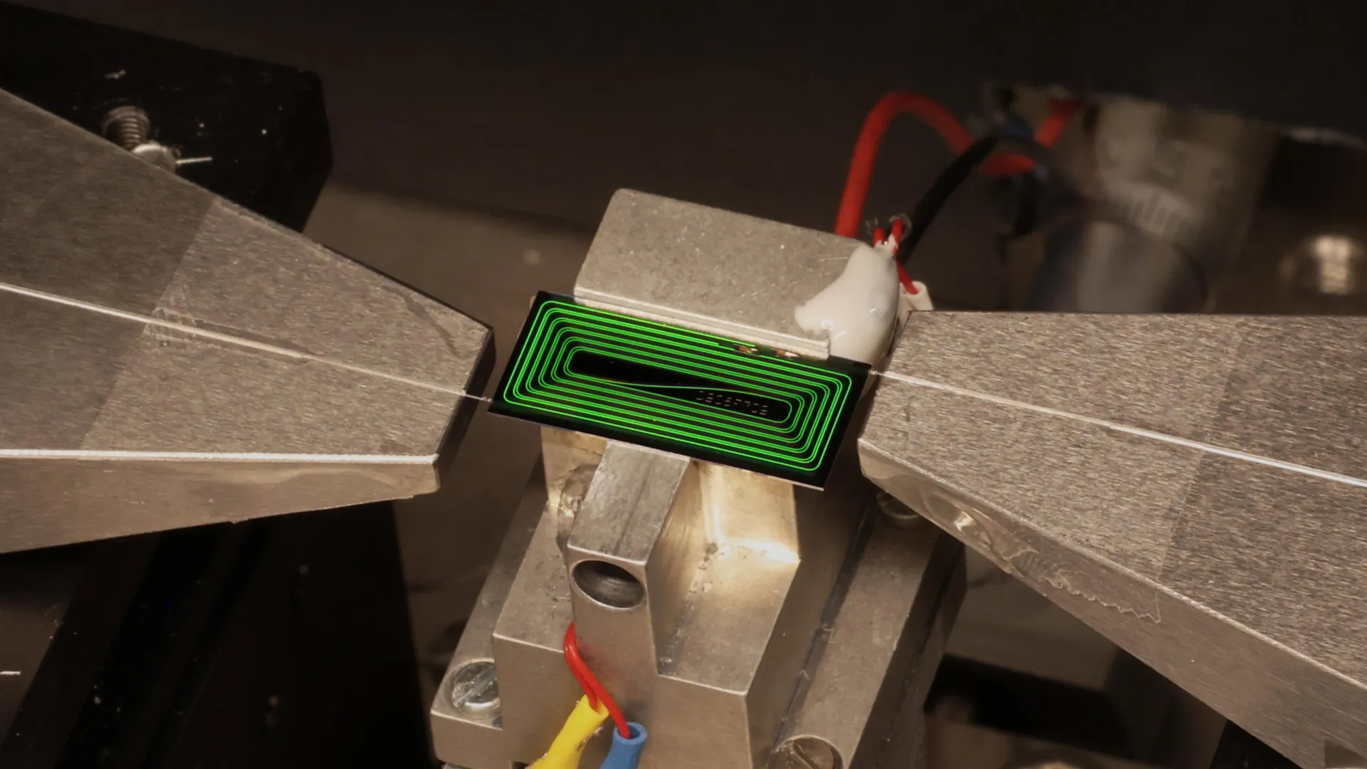
Published in the prestigious journal Nature, this breakthrough centers on a revolutionary photonic chip that packs an extraordinary technological punch. The micro-scale device delivers pulse energies of 1.05 nanojoules with pulse durations as short as 147 femtoseconds—quadrillionths of a second—achieving kilowatt-level peak powers previously restricted to room-filling equipment. By turning to an overlooked laser architecture known as the Mamyshev oscillator and adapting it to an erbium-doped silicon nitride platform, the EPFL team has cleared what was long considered the "holy grail" of integrated photonics.
This development promises to democratize ultrafast optics. Because these chips can be mass-produced using standard semiconductor manufacturing techniques, the horizon now glimmers with the prospect of affordable, portable, and ruggedized laser systems. From field-deployable environmental sensors and compact medical diagnostics to next-generation optical atomic clocks capable of revolutionizing global navigation and telecommunications, the transition of ultrafast lasers from optical benches to silicon wafers marks a watershed moment in the history of applied physics.
Detailed Chronology: The Road to the Silicon-Chip Breakthrough
To understand the magnitude of the EPFL achievement, one must trace the winding trajectory of ultrafast laser development over the past half-century. The quest to generate shorter and more intense light pulses began in earnest with the advent of mode-locking techniques in the 1960s and 1980s, which allowed lasers to emit pulses lasting picoseconds and eventually femtoseconds. These bursts of light proved transformative, allowing scientists to freeze atomic motions, observe chemical reactions in real-time, and process materials with sub-micron precision without thermal damage.
However, scaling these systems down has proven to be an engineering labyrinth. While electronic microchips successfully shrank computational hardware from room-sized mainframes to devices that fit comfortably in a trouser pocket, optics has historically resisted parallel miniaturization. Light is notoriously difficult to corral and manipulate on microscopic scales without suffering from severe scattering, diffraction, and deleterious nonlinear optical effects that degrade pulse integrity.
For more than twenty years, researchers around the globe chased the elusive goal of building a high-pulse-energy femtosecond laser directly onto a semiconductor or dielectric chip. While various iterations of on-chip continuous-wave lasers and low-power frequency combs have been successfully commercialized, creating a chip-based oscillator capable of producing high-energy, ultrashort pulses collided with a fundamental physical barrier: extreme optical confinement. When light is compressed into microscopic waveguides, its intensity skyrockets, triggering instabilities that typically tear laser pulses apart.
The turning point arrived when Professor Kippenberg’s research group—working alongside co-lead author Zheru Qiu and international collaborators—re-evaluated an older, largely bypassed laser architecture known as the Mamyshev oscillator. Originally proposed in the context of fiber lasers, the Mamyshev design relies on the interplay between spectral broadening and optical filtering to stabilize pulses, but it had received virtually zero attention within the integrated photonics community.
By redesigning the Mamyshev oscillator to function within an erbium-doped silicon nitride photonic integrated circuit, the team bypassed the complex, hard-to-fabricate components that usually plague chip-based lasers. The resulting device successfully marries the robust stability of the Mamyshev mechanism with the scalable manufacturing potential of modern microelectronics. The trajectory from a purely theoretical pursuit to a functioning, match-head-sized chip represents a masterclass in multidisciplinary engineering, bridging nonlinear optics, materials science, and semiconductor fabrication.
Supporting Context & Metrics: Inside the Technology
To appreciate how the EPFL team achieved this milestone, one must examine the intricate physics and structural architecture that govern the new device. At its core, the innovation relies on photonic integrated circuits (PICs), which manipulate light using microscopic structures called waveguides etched into a wafer substrate. Much like copper traces on a printed circuit board route electrical currents, waveguides guide, split, and filter optical signals with nanometer-scale precision.
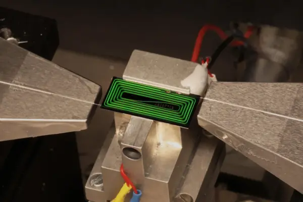
The physical blueprint of the new laser system centers on a cavity measuring 42 centimeters in total optical path length. Through sophisticated layout design, this lengthy cavity is expertly "folded" and miniaturized onto a photonic chip occupying an area roughly equivalent to a match head.
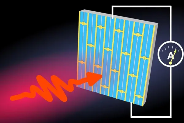
The mechanism relies on a delicate balance within the Mamyshev architecture:
- The Nonlinear Waveguide: An intense laser pulse is injected into a nonlinear waveguide positioned directly between two optical filters.
- Spectral Broadening: As the pulse traverses the waveguide, its high peak power induces nonlinear phase modulation, causing the pulse to expand into a significantly broader range of colors (frequencies).
- Filtering and Circulation: Only the portion of the light that undergoes this specific spectral broadening successfully passes through both optical filters, allowing it to continue circulating within the laser cavity.
- Suppression of Noise: Conversely, weaker background light or unwanted noise fails to broaden sufficiently, resulting in it being completely blocked by the filters and purged from the cycle.
This self-cleaning, self-stabilizing feedback loop is what sets the device apart. Photonic chips inherently confine light to extremely tight spatial dimensions, causing the optical field to interact heavily with the surrounding material. In conventional laser designs, these high optical intensities spawn unwanted nonlinearities—such as catastrophic self-phase modulation or Raman scattering—that destabilize or destroy the pulses. The Mamyshev oscillator, however, thrives on controlled nonlinearities, turning what is usually a liability into its primary stabilizing engine.
Furthermore, the choice of materials proved critical. By utilizing erbium-doped silicon nitride, the researchers leveraged a platform compatible with standard complementary metal-oxide-semiconductor (CMOS) manufacturing lines. This compatibility is the linchpin of the technology’s commercial potential. Unlike exotic crystal lasers that require meticulous hand-polishing and manual assembly, these photonic chips can be mass-produced at wafer scale.
Key Performance Metrics at a Glance:
- Pulse Duration: 147 femtoseconds (ultrashort bursts capable of capturing molecular dynamics).
- Pulse Energy: 1.05 nanojoules (sufficient energy density for industrial and medical applications).
- Peak Power: Kilowatt-level peak outputs generated from a micro-scale footprint.
- Footprint: A laser cavity folded onto a chip the size of a match head, replacing optical tables that span several square meters.
- Scalability: Wafer-scale fabrication yields exceeding 1,000 laser cavities simultaneously on a single substrate.
Official Statements & Expert Perspectives
The breakthrough has generated substantial excitement within the global physics and engineering communities, signaling a paradigm shift in how high-performance optics will be deployed in the coming decades.
Reflecting on the two-decade quest to realize this technology, Professor Tobias J. Kippenberg articulated the depth of the achievement:
"For more than twenty years, a high-pulse-energy femtosecond laser on a chip was widely regarded as a holy grail of integrated photonics. Our result shows that it is not only possible, but that it can be achieved with a surprisingly elegant architecture that the integrated-photonics community had overlooked."
The elegance of the design lies in its manufacturing simplicity—a factor emphasized by Zheru Qiu, co-lead author of the research publication. By sidestepping components that are notoriously difficult to fabricate on microscopic scales, the team has engineered a system primed for industrial adoption.
"This design is especially attractive because it does not require any component that is difficult to make on this erbium-doped silicon nitride chip," explains Qiu. He further highlights the practical implications of utilizing the Mamyshev oscillator to tame optical instabilities: "Photonic chips confine light to extremely small waveguides, causing light to interact strongly with itself. In many laser architectures, these nonlinear effects can destabilize the laser pulses. The Mamyshev oscillator, however, is far less susceptible to these problems, making it particularly well suited for integrated photonic devices."
Looking toward the commercial and applied horizons, Qiu underscores the transformative capability of the device’s output:
"With kilowatt-level peak powers, the chip can drive demanding applications that have long depended on large, expensive laboratory lasers."
The collaborative nature of the research—spanning the EPFL Institute of Electrical and Microengineering and the Helmholtz-Zentrum Dresden-Rossendorf (HZDR)—underscores the cross-disciplinary synergy required to push modern photonics across the threshold from academic curiosity to deployable technology.
Future Outlook: A New Era for Field-Ready Optics
The miniaturization of ultrafast lasers from room-filling optical tables to match-head-sized silicon chips opens a sweeping landscape of commercial, industrial, and scientific possibilities. By radically reducing the size, weight, power consumption, and cost (SWaP-C) profile of femtosecond laser systems, this breakthrough bridges the gap between delicate laboratory instrumentation and ruggedized field deployment.
1. Environmental Monitoring and Pollution Detection
Traditional spectroscopy setups used to detect trace atmospheric pollutants or greenhouse gases often rely on delicate, rack-mounted optical parametric oscillators and femtosecond sources. The advent of wafer-scale, chip-based ultrafast lasers paves the way for handheld environmental monitors. These devices could be deployed on autonomous drones, weather balloons, or fixed urban sensor nodes to perform real-time, highly sensitive trace-gas analysis and atmospheric composition profiling.
2. Advanced Materials Science and Industrial Non-Destructive Testing
In manufacturing sectors, micro-machining, cutting, and quality control demand absolute precision. Compact ultrafast lasers integrated directly into robotic arms or portable inspection units could perform high-resolution optical coherence tomography (OCT) and non-destructive testing on-site. Manufacturers would be able to detect hidden structural defects, micro-fractures, or material fatigue in aerospace components and semiconductor packaging without transporting samples to specialized analytical laboratories.
3. Portable Medical Diagnostics and Therapeutics
While ultrafast lasers are already staples in specialized eye surgery (such as LASIK) and multiphoton microscopy, their bulk has restricted their use to advanced clinical centers. Scaled-down, cost-effective semiconductor lasers could dramatically decentralize diagnostic medicine. Portable dermatological scanners, compact multi-photon tissue imagers for early cancer detection, and ultra-precise surgical tools could become standard equipment in rural clinics, ambulances, and field hospitals worldwide.
4. Next-Generation Optical Atomic Clocks and Navigation
Optical frequency combs—the Nobel Prize-winning technology powered by ultrafast lasers—form the beating heart of the world’s most accurate atomic clocks, which lose less than a second over billions of years. However, their reliance on complex tabletop lasers has limited their utility outside metrology laboratories. Integrating the core laser source onto a robust photonic chip brings humanity one step closer to compact, field-deployable optical clocks. Such devices could provide unprecedented timing synchronization for secure telecommunications networks, deep-space exploration, and GPS-independent navigation systems resilient against electronic jamming.
As the EPFL team and their collaborators continue to refine the fabrication processes and explore mass-production pathways, the transition of ultrafast optics from benchtop to chip-scale is no longer an idealized horizon—it is an unfolding reality. With thousands of laser cavities poised to roll off semiconductor foundry lines simultaneously, the next revolution in light-based technology is set to fit right in the palm of your hand.