










Executive Overview
For decades, the electromagnetic spectrum has been thoroughly mapped, utilized, and commercialized across almost all of its domains—from radio waves and microwaves to infrared, visible light, ultraviolet, X-rays, and gamma rays. Yet, nestled stubbornly between the microwave and infrared bands lies a notoriously difficult frontier: the terahertz (THz) frequency range.
Often referred to as the "terahertz gap," this spectral region holds immense promise for next-generation applications, including ultra-high-speed wireless communications, non-invasive medical diagnostics, advanced security screening, biomedical sensing, and industrial quality control. However, harnessing terahertz radiation has historically been hindered by the limitations of available hardware. Existing detectors are frequently sluggish, insufficiently sensitive, or dependent on bulky, expensive infrastructure that requires extreme cryogenic cooling to function reliably.
Now, a team of international researchers has shattered these long-standing barriers. By forging an innovative marriage between quantum physics and advanced materials engineering, the team has developed a compact, highly efficient terahertz detector. Published recently in the prestigious journal Advanced Photonics, the breakthrough relies on a novel quantum mechanism paired with a specially engineered metasurface.
This hybrid architecture bypasses the traditional efficiency bottlenecks of conventional light-detection systems. By concentrating incoming radiation into microscopic detection channels embedded directly within a patterned metasurface, the new device achieves a staggering twenty-fold improvement in external quantum efficiency compared to its predecessors. Operating entirely at zero bias—thereby eliminating noise-generating dark currents—this semiconductor-friendly innovation points the way toward scalable, highly integrated, and field-deployable terahertz technologies.
Detailed Chronology: The Evolution of a Quantum Breakthrough
The journey toward this milestone was not forged overnight; it represents the culmination of years of meticulous inquiry into low-dimensional physics, semiconductor manufacturing, and sub-wavelength optics.
Phase I: Recognizing the Terahertz Bottleneck
The genesis of the project lay in the well-documented shortcomings of prevailing terahertz detection paradigms. Traditional thermal detectors (such as bolometers) and electronic mixers have long struggled with trade-offs between speed, sensitivity, and operational complexity. While quantum-based photoelectric detectors offered theoretical advantages, they typically suffered from low absorption rates because individual antenna elements could only capture a tiny fraction of incoming, highly diffractive terahertz waves.
Researchers at the University of Cambridge’s renowned Cavendish Laboratory, working alongside collaborators, turned their attention to an alternative quantum phenomenon: the in-plane photoelectric effect. In this process, incoming photons transfer their energy directly to electrons confined within a two-dimensional electron gas (2DEG). When energized, these electrons cross a carefully engineered potential step, generating a measurable electrical current.
While earlier iterations of Photoelectric Tunable-Step (PETS) detectors proved the viability of this mechanism, they remained hobbled by poor optical coupling. They simply could not gather enough light to make the quantum mechanism practical for widespread commercial or scientific deployment.
Phase II: The Metasurface Solution
To solve the light-collection dilemma, the research team looked to metasurfaces—artificially engineered, two-dimensional structures patterned with sub-wavelength features that can manipulate electromagnetic waves in unconventional ways. Rather than treating light collection and detection as two separate engineering problems (the traditional approach of pairing a detector with an external lens or bulky antenna), the team decided to integrate the two disciplines into a single, cohesive architecture.
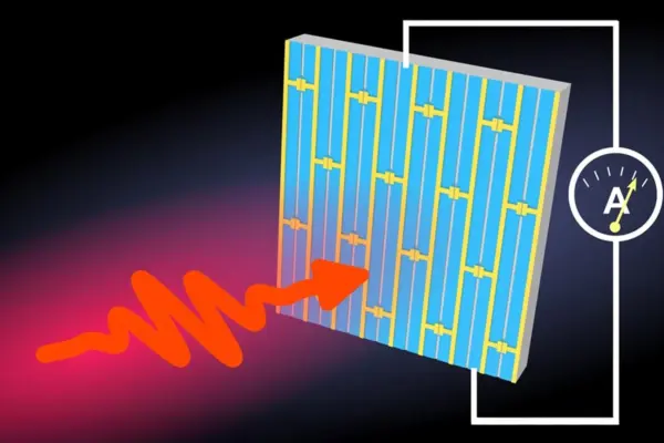
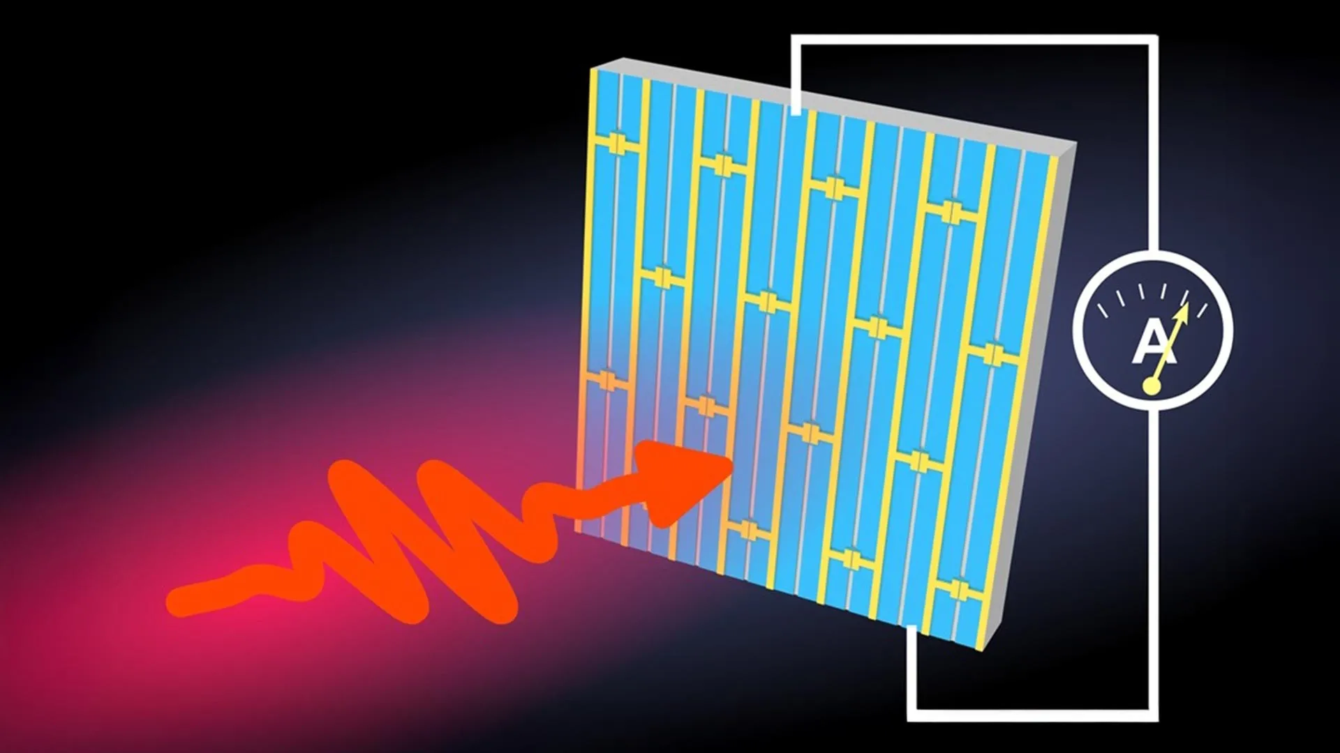
Led by corresponding author Wladislaw Michailow—who initiated the research at the University of Cambridge before transitioning to Swansea University—the team designed a repeating "brickwork" pattern. This geometric configuration serves a dual purpose: it acts as an optical collector that captures incoming terahertz radiation, and it functions as a focusing lens that channels that energy into extremely narrow, capacitive gaps.
Phase III: Fabrication and Testing
With the blueprint optimized via rigorous computer simulations—fine-tuning gap dimensions, structural spacing, and electron channel widths to maximize field enhancement—doctoral researcher Ruqiao Xia undertook the delicate task of manufacturing and measuring the devices.
Fabricated using advanced semiconductor processing techniques analogous to those used for standard field-effect transistors (FETs), the resulting chips featured individual PETS detection elements embedded directly inside the metasurface’s capacitive gaps. This ensured optimal electromagnetic coupling between the light-concentrating structure and the quantum detection elements.
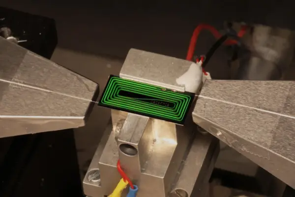
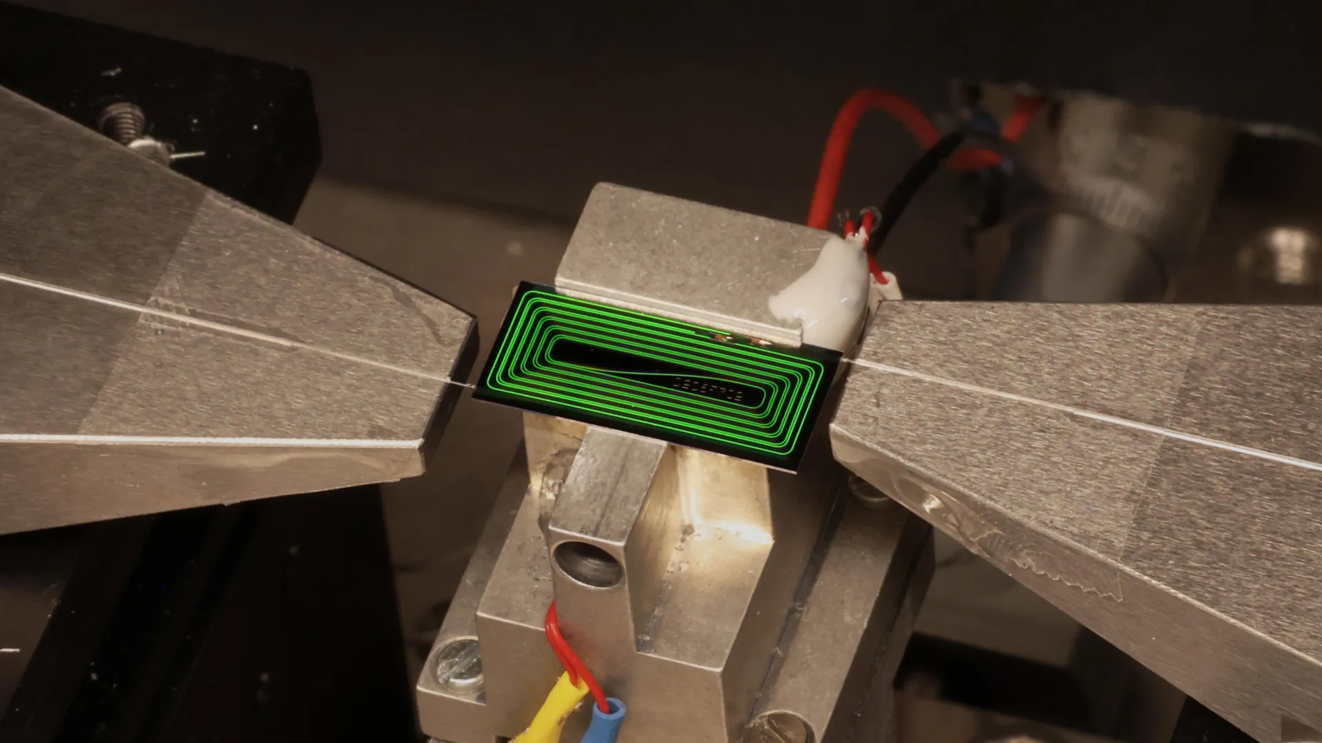
Upon cooling the proof-of-concept device to 10 Kelvin—a temperature easily achievable with compact, closed-cycle cryocoolers rather than expensive liquid helium—the researchers exposed it to radiation at approximately 1.9 THz. The detector responded immediately, producing a clean, sharp electrical signal that precisely mirrored the modulation pattern of the incoming radiation.
Supporting Context & Metrics: Quantifying the Leap in Performance
The quantitative results of the Cambridge-led study underscore a monumental leap forward for terahertz detector design. In the world of semiconductor physics and optoelectronics, incremental gains of 5% or 10% are standard; a twenty-fold performance leap is transformative.
Key Performance Metrics
- External Quantum Efficiency: The proof-of-concept device achieved an external quantum efficiency of 2.1 percent at 1.9 THz. This represents an approximate 20-fold improvement over previously demonstrated PETS detector designs.
- Responsivity: Standardized measurements revealed a robust responsivity of 2.7 amperes per watt (A/W), proving that the device efficiently translates captured photons into usable electrical current.
- Zero-Bias Operation: Because the device operates with zero source-drain bias, it fundamentally eliminates dark currents—the steady, unwanted background electrical noise that plagues many semiconductor detectors and degrades signal-to-noise ratios.
- Operating Temperature: Tested at 10 K, the detector architecture is fundamentally compatible with compact, mechanical cryocoolers. This bypasses the need for cumbersome liquid helium setups, bringing high-sensitivity quantum detection closer to practical, field-ready deployment.
The Mechanics of the Metasurface Advantage
To understand why these metrics are so impressive, one must examine the physics of terahertz waves. Terahertz radiation occupies wavelengths longer than infrared light but shorter than microwaves (roughly 300 gigahertz to 3 terahertz). Because of these relatively long wavelengths, focusing terahertz light using conventional refractive optics (like glass or silicon lenses) requires bulky components that are difficult to align and prone to diffraction losses.
By embedding the detection elements directly within the capacitive gaps of a planar metasurface, the researchers effectively turned the detector’s surface into its own optical system. The brickwork pattern traps the electric field, concentrating it intensely within the exact spatial regions where the 2DEG is primed to absorb it. Consequently, 100% of the concentrated energy is funneled directly into signal generation, eliminating the optical dead zones that crippled earlier planar designs.
Furthermore, because the entire structure is fabricated on a semiconductor platform using standard planar lithography, the manufacturing workflow is inherently scalable. The device geometry can be adjusted parametrically, meaning the underlying physical principles can theoretically be tuned to target other spectral bands, spanning from microwaves to mid-infrared wavelengths.
Official Statements and Expert Insights
The implications of this research extend far beyond the confines of academic physics, promising to unlock new commercial capabilities across a diverse array of industries.
Reflecting on the integration of the metasurface and the quantum detector, corresponding author Wladislaw Michailow emphasized the elegance of the design:
"This ensures optimal coupling of the metasurface to the detection elements. Compared to the conventional approach of connecting multiple devices in parallel, this approach allowed us to significantly boost the detection sensitivity."
Detailing the electrical behavior and the minimization of noise, lead fabricator Ruqiao Xia, who conducted the experimental work as part of her doctoral research in the Semiconductor Physics Group at the Cavendish Laboratory, noted:
"The devices are direct detectors operating at zero bias, and therefore, they operate without dark currents."
Looking at the broader technological horizon, David Ritchie, head of the Semiconductor Physics Group at the University of Cambridge and co-author of the study, highlighted the vast commercial and scientific potential that uninhibited terahertz detection can unlock:
"The results are particularly intriguing due to the applications that terahertz technology can enable, in areas such as wireless networks, healthcare, astronomy, biomedicine, quality assurance in manufacturing, and many others."
Future Outlook: Unlocking the Terahertz Frontier
The successful demonstration of a quantum metasurface photodetector based on a two-dimensional electron system marks a watershed moment for electromagnetic engineering. By dismantling the traditional dichotomy between light collection optics and quantum detection elements, this research opens several exciting pathways for future development.
1. Scaling and Frequency Tuning
Because the architecture relies on scalable geometric patterns rather than fixed bulk optics, future iterations of the technology could be engineered to span a wider continuous frequency range. Researchers plan to investigate how modifications to the metasurface unit cells can optimize absorption for higher or lower terahertz bands, as well as adjacent infrared and microwave spectrums.
2. Room-Temperature Operations and Compact Cooling
While the current proof-of-concept device operates at 10 K, the underlying physics of the in-plane photoelectric effect do not fundamentally preclude higher-temperature functionality. Ongoing materials research aims to optimize the potential step heights and electron mobility within alternative semiconductor material systems. Achieving efficient operation at temperatures accessible via thermoelectric coolers or standard Stirling cryocoolers would eliminate cryogenic dependencies entirely, paving the way for handheld, portable terahertz imagers.
3. System-on-Chip Integration
Perhaps the most profound commercial advantage of the planar metasurface detector is its compatibility with standard semiconductor fabrication lines. Because the detectors can be manufactured using established microelectronics processes, they can be monolithically integrated with on-chip readout circuitry, amplifiers, and signal-processing units. This opens the door to dense, multi-pixel terahertz focal-plane arrays—essentially "terahertz cameras"—capable of real-time imaging without the need for complex external lens assemblies or manual optical alignment.
4. Real-World Applications on the Horizon
With improved sensitivity, elimination of dark current, and a compact footprint, the applications envisioned by the Cambridge team are rapidly moving from theoretical conjecture to practical reality:
- Telecommunications: As 6G wireless standards look to utilize sub-terahertz and terahertz frequency bands to achieve data rates hundreds of times faster than current 5G networks, highly sensitive, low-noise detectors will be vital receiver components.
- Biomedicine and Healthcare: Terahertz radiation is non-ionizing, making it safe for biological tissue imaging. Improved detectors could enable real-time, non-invasive skin cancer detection, dental diagnostics, and molecular sensing.
- Industrial Quality Assurance: Terahertz waves can penetrate packaging, plastics, and ceramics, allowing manufacturers to inspect internal structures, detect hidden defects, or verify pharmaceutical tablet compositions on high-speed production lines without opening packaging.
- Security and Defense: Advanced passive and active terahertz scanners can detect concealed weapons, explosives, or contraband under clothing or inside cargo containers with high spatial resolution.
Conclusion
The creation of this quantum-metasurface hybrid detector proves that the most stubborn technological bottlenecks can often be solved not by building bigger and more expensive machines, but by looking closer at the fundamental physics of materials. By merging quantum electron dynamics with sub-wavelength optical engineering, the research team at the University of Cambridge has turned the "terahertz gap" from an insurmountable chasm into an open door. As this technology matures and scales toward commercial manufacturing, it promises to illuminate one of the final dark corners of the electromagnetic spectrum.