










Executive Overview
For decades, the electromagnetic spectrum has been thoroughly mapped, harnessed, and industrialized, with scientists and engineers deploying sensors capable of capturing everything from high-energy gamma rays to low-frequency radio waves. Yet, a stubborn middle child of the spectrum has consistently resisted easy exploitation: the terahertz (THz) band. Nestled precisely between microwaves and infrared light, terahertz radiation holds immense theoretical promise. It possesses the unique ability to penetrate numerous non-conducting materials like plastics, clothing, and packaging while offering spatial resolution far superior to standard microwaves. These traits make the THz band an unprecedented goldmine for next-generation wireless communications, biomedical imaging, non-destructive manufacturing quality control, and advanced security screening.
Despite these tantalizing applications, practical utilization of terahertz waves has been severely bottlenecked by a fundamental hardware limitation. Traditional detectors operating within this frequency range are notoriously sluggish, lack the requisite sensitivity to capture faint signals, or depend on bulky, cumbersome equipment that demands extreme cryogenic cooling to function. They have historically been expensive to build, difficult to calibrate, and nearly impossible to integrate smoothly into compact, on-chip electronic architectures.
Now, a team of international researchers has shattered these long-standing barriers. In a breakthrough published in the journal Advanced Photonics, scientists have unveiled a novel, highly compact terahertz detector that ingeniously marries advanced quantum mechanics with specially engineered metasurfaces. This hybrid approach has yielded a staggering twenty-fold improvement in external quantum efficiency compared to preceding iterations.
By eliminating the need for external focusing lenses, suppressing dark current through a zero-bias architecture, and concentrating radiation directly into the active quantum regions of a semiconductor chip, this discovery signals a paradigm shift. It paves the way for scalable, highly responsive, and semiconductor-compatible terahertz systems that could soon transition from specialized laboratory curiosities into ubiquitous industrial and consumer tools.
Detailed Chronology: The Evolution of a Quantum Breakthrough
The journey toward this technological leap did not happen overnight; it is the culmination of years of iterative research in semiconductor physics, quantum confinement, and nanophotonics.
The Theoretical Foundation: The In-Plane Photoelectric Effect
To understand the significance of the recent breakthrough, one must look at the underlying physics. Conventional photodetectors rely on vertical carrier excitation, a process wherein incoming photons must possess enough energy to exceed a strict minimum threshold (the bandgap), hoisting electrons across an energetic barrier. In the terahertz regime, however, photon energies are exceptionally low, making this traditional mechanism inefficient or entirely non-viable.
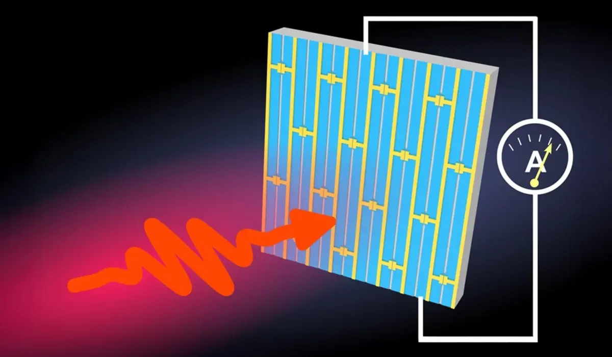
To bypass this roadblock, researchers turned to the in-plane photoelectric effect. In this quantum mechanism, incoming terahertz photons transfer their momentum and energy directly to electrons confined within a two-dimensional electron gas (2DEG). These energized electrons are coaxed into crossing a carefully engineered potential step—a photoelectric tunable-step (PETS)—generating a measurable electrical current.
While this in-plane approach was a major theoretical victory because it discarded energy threshold limitations, early implementations suffered from a critical flaw. Because these detectors relied on individual antenna elements to capture light, they could only harvest a minuscule fraction of the ambient terahertz radiation. The vast majority of the signal simply bounced off or bypassed the active area entirely.
Introducing the Metasurface Solution
Recognizing that individual antennas were a dead end for high-efficiency capture, the research team—led by Wladislaw Michailow, then at the University of Cambridge and subsequently at Swansea University—pivoted toward nanophotonics. They decided to integrate the quantum detection elements directly into a metasurface: a two-dimensional, artificially engineered optical surface patterned with sub-wavelength structures designed to manipulate electromagnetic waves in unprecedented ways.
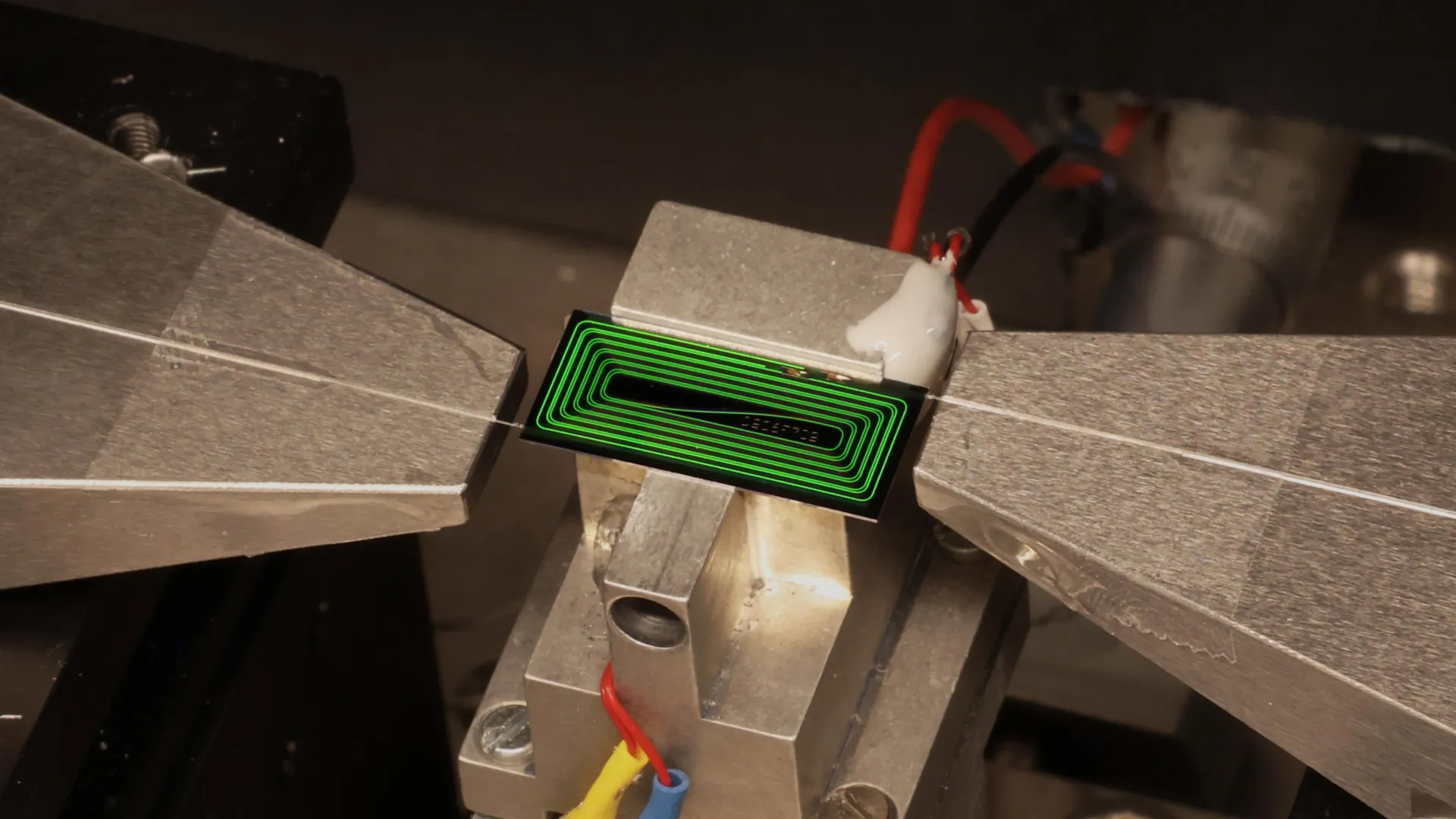
Instead of treating light collection and electronic detection as two separate engineering problems (where light is first gathered by a lens or mirror and then routed to a detector), the team fused the two systems into a unified architecture. They designed a repeating "brickwork" pattern across the semiconductor surface. This geometric layout performed a dual function: it acted as an efficient optical antenna array that trapped and channeled incoming terahertz radiation, and it concentrated that trapped energy into ultra-narrow capacitive gaps where the detection process actually occurred.
Simulation, Fabrication, and Testing
With the conceptual framework established, the researchers utilized advanced computer simulations to meticulously optimize structural parameters. Every dimension—from the precise width of the capacitive gaps to the spacing between repeating units—was tuned to maximize electric field confinement without choking the electron channel.
Fabricated using standard semiconductor manufacturing techniques akin to those employed for field-effect transistors (FETs), the resulting device was ready for empirical validation. Led by doctoral researcher and first author Ruqiao Xia within the Semiconductor Physics Group at Cambridge’s Cavendish Laboratory, the team cooled the prototype to 10 Kelvin—a temperature easily achieved using compact, low-maintenance commercial cryocoolers rather than complex liquid helium systems.
When exposed to radiation at approximately 1.9 terahertz, the detector produced an instantaneous, pristine electrical response that mirrored the on-off modulation of the incoming beam with remarkable fidelity.
Supporting Context & Metrics: Decoding the Performance Gains
The empirical results recorded during the testing phase validate the efficacy of combining quantum 2DEG systems with metasurfaces. The metrics achieved by the research team represent a quantum leap over previous generations of terahertz sensors.
Quantitative Breakdown
- Responsivity: The proof-of-concept detector achieved a high responsivity of 2.7 amperes per watt (A/W), demonstrating exceptional conversion efficiency from optical photon input to electrical output signal.
- External Quantum Efficiency (EQE): At a test frequency of 1.9 THz, the device registered an EQE of 2.1 percent. When compared directly against previously demonstrated PETS detectors, this figure marks a twenty-fold performance enhancement.
- Thermal Operating Profile: By operating successfully at temperatures achievable via compact cryocoolers (tested at 10 K, with architectures pointing toward higher operational thresholds), the design bridges the frustrating gap between hyper-sensitive, liquid-helium-dependent cryogenic detectors and sluggish, noisy room-temperature alternatives.
- Bias and Noise Reduction: A crucial metric for sensor utility is signal-to-noise ratio. Because this detector operates with zero source-drain bias, it is entirely free of "dark current"—the persistent background electrical noise that plagues biased detectors and obscures weak signals. The output current is driven purely by the photoelectric phenomenon induced by the captured photons.
Architectural Advantages Over Legacy Systems
| Feature | Traditional THz Detectors | New Quantum Metasurface Detector |
|---|---|---|
| Light Collection | Relies on bulky external lenses, mirrors, or discrete antennas | Integrated metasurface "brickwork" pattern concentrates light intrinsically |
| Energy Thresholds | Often constrained by strict bandgap energy requirements | Zero threshold requirement via the in-plane photoelectric effect |
| Electrical Noise | Susceptible to dark current due to mandatory operating bias | Zero-bias operation completely eliminates dark current |
| Integration Potential | Difficult to scale; requires complex optical alignment | Compatible with standard semiconductor manufacturing (CMOS/FET-like) |
| Form Factor | Bulky, heavy, and reliant on complex optical setups | Compact, flat-profile, and easily integrated onto microchips |
Official Statements from the Research Leadership
The implications of this breakthrough extend far beyond academic novelty, touching on fundamental shifts in how optical and electronic systems can be co-designed.
Reflecting on the integration methodology, corresponding author Wladislaw Michailow emphasized the synergy between the optics and the electronics:
"Rather than designing the detector and light-collection system separately, we began with the metasurface itself and built the detection elements directly into regions where the electric field is strongest. This ensures optimal coupling of the metasurface to the detection elements. Compared to the conventional approach of connecting multiple devices in parallel, this approach allowed us to significantly boost the detection sensitivity."
Detailing the electrical behavior and the complete absence of unwanted background interference, first author Ruqiao Xia noted:
"The devices are direct detectors operating at zero bias, and therefore, they operate without dark currents. The patterned metasurface captures a larger fraction of incoming radiation and focuses it directly into the detector’s active regions, allowing us to achieve unprecedented conversion efficiency without introducing thermal or electrical noise from an external power supply."
Looking toward the broad societal and industrial horizons opened by the technology, co-author David Ritchie, head of the Semiconductor Physics Group at the Cavendish Laboratory, highlighted the vast array of impending use cases:
"The results are particularly intriguing due to the applications that terahertz technology can enable, in areas such as wireless networks, healthcare, astronomy, biomedicine, quality assurance in manufacturing, and many others."
Future Outlook: Paving the Way for Commercial Terahertz Integration
As the scientific community digests the implications of this study, the roadmap for future development is already taking shape. The successful demonstration of a quantum metasurface photodetector based on a two-dimensional electron gas opens multiple avenues for commercialization and technological scaling.
Scalability and Frequency Agnosticism
One of the most potent advantages of the team’s geometric design is its inherent scalability. Because the operational physics are governed by structural dimensions and quantum mechanical principles within a planar semiconductor layout, the core architecture is not strictly locked to the 1.9 THz sweet spot. By altering the geometric scale of the metasurface units, future iterations of the detector could theoretically be tuned to operate seamlessly across a vast continuum of the electromagnetic spectrum—stretching downward into microwave frequencies or upward into the mid-infrared range.
Streamlining Manufacturing and Deployment
In the realm of commercial electronics, manufacturing feasibility dictates market adoption. Because the fabrication processes mirror well-established semiconductor manufacturing techniques used for field-effect transistors, the transition from academic lab bench to commercial foundry is remarkably straightforward.
Furthermore, the elimination of external focusing optics—such as bulky silicon lenses that require painstaking mechanical alignment—slashes production costs, reduces device weight, and shrinks the overall footprint. Flat-profile detectors can be surface-mounted directly onto electronic circuit boards, paving the way for monolithic, multi-pixel terahertz imaging cameras and high-density transceiver arrays.
Toward Room-Temperature Viability
While the initial proof-of-concept tests were conducted at 10 Kelvin, the engineering principles embedded within the device design point toward eventual operation at significantly warmer temperatures. Already, similar PETS architectures have shown viability at temperatures accessible via compact, solid-state cryocoolers rather than massive liquid helium tanks. As materials science marches forward—incorporating higher-mobility 2DEG systems and novel heterostructures—the holy grail of a fully room-temperature, highly sensitive terahertz detector moves closer to reality.
Transforming Industry Sectors
When these detectors mature into commercial products, their impact will be felt across diverse industries:
- Telecommunications: As 6G wireless networks eye the terahertz spectrum for ultra-high-bandwidth data transmission, compact and sensitive detectors will be required at every receiving node.
- Biomedicine & Healthcare: Non-invasive diagnostic tools utilizing terahertz waves could image superficial tissues, monitor hydration levels, or detect cancerous cells with high molecular specificity, all without harmful ionizing radiation.
- Manufacturing & Quality Assurance: Factory floors will be able to perform real-time, non-destructive internal scans of composite materials, pharmaceuticals, and electronics packaging to catch microscopic defects before products ship.
- Security: Advanced standoff imaging systems will easily detect concealed weapons, explosives, or contraband through packaging and garments with unprecedented clarity.
By successfully bridging the gap between quantum mechanics, nanophotonics, and scalable semiconductor manufacturing, this research has transformed terahertz detection from an unwieldy laboratory challenge into a sleek, highly efficient technology poised to redefine how humanity interacts with the invisible spectrum.