










AUSTIN, Texas — In a strategic move set to reshape manufacturing paradigms across the global electronics sector, Austin-based Electroninks and Japan-headquartered SIIX Corporation have announced a major expansion of their collaborative efforts. The partnership focuses on accelerating the commercialization and deployment of additive, high-frequency electromagnetic interference (EMI) shielding solutions.
This expanded alliance bridges the gap between advanced materials science and large-scale electronics manufacturing services (EMS). By integrating Electroninks’ proprietary metal-organic decomposition (MOD) conductive ink platform with SIIX’s newly established, specialized ultrasonic spray coating infrastructure, the two companies are empowering original equipment manufacturers (OEMs) to overcome critical engineering bottlenecks. As modern electronic devices operate at increasingly higher frequencies and component densities, this collaboration offers a scalable, lightweight, and highly adaptable path forward for industries ranging from automotive systems to advanced consumer electronics and semiconductor packaging.
Executive Overview
The convergence of high-frequency communications, vehicle electrification, and miniaturized consumer electronics has transformed EMI shielding from a routine component-level design consideration into a complex, system-level engineering hurdle. Traditional methods of shielding—such as heavy stamped metal cans, electroplated plastic enclosures, and bulky mechanical barriers—introduce significant weight, manufacturing complexity, and design constraints.
To address these challenges, Electroninks and SIIX are scaling an additive manufacturing approach that deposits precision conductive coatings directly onto complex, three-dimensional geometries. Under the terms of the expanded agreement, SIIX has established a dedicated spray coating environment utilizing state-of-the-art ultrasonic equipment. This setup is purpose-built to facilitate comprehensive prototype trials, process optimization, and collaborative material testing for customers in Japan and international markets.
Rather than offering a rigid, one-size-fits-all manufacturing process, the partnership emphasizes a joint engineering framework. Electroninks provides its cutting-edge MOD material science and formulation expertise, while SIIX leverages its vast EMS footprint and production know-how. Together, they work directly alongside customers to evaluate, iterate, and validate custom coating processes—beginning at the prototyping stage and building a clear pathway toward seamless high-volume production.
Detailed Chronology and Operational Evolution
The expansion of the Electroninks-SIIX relationship represents the culmination of years of targeted technological development and strategic alignment between the two organizations.
Laying the Groundwork: Material Science Meets EMS
Electroninks established its reputation as a pioneer in advanced metal complex inks, developing proprietary formulations utilizing silver, gold, platinum, nickel, and copper. These MOD inks deliver exceptional conductivity, low curing temperatures, and high compatibility with additive deposition techniques. Recognizing the immense potential for these materials in mainstream manufacturing, Electroninks sought a Tier-1 EMS partner with the operational scale and technical acumen to bring additive electronics out of the laboratory and onto the factory floor.
SIIX Corporation, a prominent global manufacturing services provider with extensive operations across Asia and worldwide, emerged as an ideal collaborator. Over successive phases of engagement, the two companies identified high-frequency EMI shielding as an immediate, high-impact application for additive manufacturing technologies.
Establishing the Specialized Ultrasonic Spray Environment
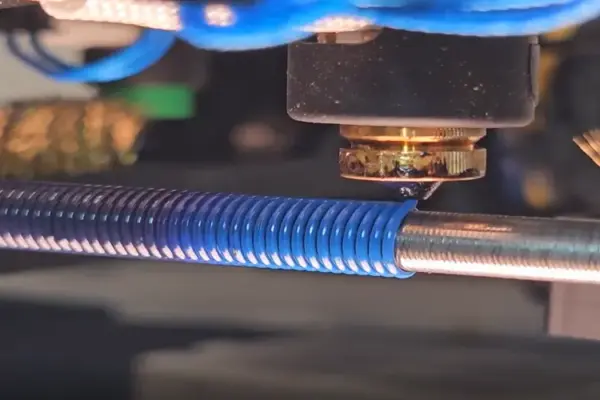
A major milestone in the current phase of the partnership is SIIX’s installation and operationalization of advanced spray coating equipment within a specialized ultrasonic spray environment. Ultrasonic coating technology is critical for additive electronics because it produces a highly uniform, controlled thin-film deposition, even when applied to complex 3D surfaces, internal cavities, and challenging substrate materials.
By stationing this specialized environment within its facilities, SIIX has eliminated a major barrier to entry for prospective customers. OEMs can now bring their specific component designs—including common automotive plastics such as polybutylene terephthalate (PBT)—to SIIX for hands-on prototyping. This allows engineers to assess the efficacy of additive EMI shielding on actual hardware rather than relying on theoretical simulations or generalized coupons.
Collaborative Process Development Framework
The partnership rejects the traditional vendor-customer dynamic in favor of a collaborative co-development model. When an OEM engages with Electroninks and SIIX, the teams do not assume that process parameters are pre-optimized. Instead, they jointly establish:
- Spray Parameters: Fine-tuning atomization rates, traverse speeds, and nozzle distances for specific geometries.
- Curing Profiles: Optimizing thermal parameters to ensure maximum conductivity without compromising heat-sensitive underlying substrates.
- Material Compatibility: Testing and validating MOD ink formulations against specific customer-selected resins, plastics, and composite materials.
Furthermore, the companies have instituted a structured framework designed to continuously integrate newly developed Electroninks materials into the testing pipeline. As Electroninks expands its portfolio of conductive inks, SIIX’s specialized environment enables rapid iteration, ensuring that customers gain immediate access to the latest material advancements.
Supporting Context, Technological Drivers, and Market Metrics
The urgency behind the Electroninks-SIIX collaboration is driven by fundamental shifts in electronics architecture across multiple vertical markets.
The Automotive Revolution: ECUs, PCUs, and Beyond
The rapid transition toward Software-Defined Vehicles (SDVs), Advanced Driver-Assistance Systems (ADAS), and full electric vehicle (EV) architectures has drastically increased the density of semiconductor components inside automobiles. Electronic Control Units (ECUs), Power Control Units (PCUs), and battery management systems operate at high switching frequencies while residing in tightly packed spaces.
In these environments, electromagnetic interference can disrupt critical safety systems, sensor arrays, and infotainment networks. Traditional metal enclosures add dead weight to vehicles, counteracting efforts to maximize driving range and energy efficiency. By utilizing Electroninks’ precision spray-coated MOD inks, manufacturers can deposit conformal shielding directly onto plastic housings. This approach slashes component weight, simplifies assembly, eliminates secondary mechanical fasteners, and provides superior high-frequency shielding performance.

Beyond Automotive: Consumer Electronics and Semiconductor Packaging
While automotive applications represent an initial focal point, the utility of additive EMI shielding spans a vast array of industries. Modern wearable technology, medical monitoring devices, IoT sensors, and high-performance computing modules demand ultra-compact designs that defy traditional shielding methodologies.
Moreover, as semiconductor packaging trends toward advanced 2.5D and 3D architectures, the need for localized, sub-millimeter shielding within packages becomes paramount. Electroninks’ metal complex inks—which offer high-resolution printing and compatibility with semiconductor manufacturing lines—position the company at the bleeding edge of microelectronics packaging innovation. To support this rising tide of demand, Electroninks has concurrently upgraded its own internal infrastructure, installing advanced spray and printing systems at its facilities to enhance manufacturing consistency and prepare for long-term global scale-up.
Official Statements and Industry Perspectives
Leadership from both organizations underscored the transformative nature of the expanded collaboration and its strategic importance for the global electronics supply chain.
"As electronics across automotive and many other industries become denser and operate at higher frequencies, EMI shielding is evolving from a component-level consideration into a system-level engineering challenge," said Takashi Mochizuki, Director of Sales and Business Development at Electroninks.
"This collaboration brings together advanced conductive materials, a specialized ultrasonic spray coating environment, and global manufacturing expertise so we can work directly with customers to establish coating processes suited to their products, from automotive electronics to a broad range of other applications."
The synergy between advanced material properties and scalable manufacturing execution was further emphasized by the executive leadership team at Electroninks.
"Additive manufacturing is enabling entirely new approaches to electronics integration," added Melbs LeMieux, Co-founder and President at Electroninks.
"By combining advanced materials with scalable EMS manufacturing, SIIX—a longtime partner of Electroninks—is now taking a strong initiative to advance their EMS business and offer their customers advancements in functionality and production times. We are proud to support SIIX and the overall market in Japan as they look to adopt MOD technology in their electronics manufacturing supply chains."
Future Outlook and Strategic Roadmap
Looking ahead, Electroninks and SIIX expect their partnership to serve as a catalyst for broader adoption of additive manufacturing within mainstream electronics production. The current phase—focused heavily on prototyping, material optimization, and process validation in Japan—is designed to lay a robust foundation for commercial manufacturing deployments.
As customer adoption matures, the collaborative framework is anticipated to scale geographically, extending into additional manufacturing regions and integration hubs managed by SIIX. Furthermore, the partnership serves as a living laboratory for future material workflows, paving the way for the introduction of next-generation conductive inks tailored for emerging semiconductor packaging paradigms and ultra-high-frequency telecommunications infrastructure.
By dismantling traditional manufacturing barriers and proving the commercial viability of additive EMI shielding at scale, Electroninks and SIIX are not merely supplying components—they are actively architecting the production standards of tomorrow’s electronic landscape.
About Electroninks
Electroninks Incorporated is a world leader in the commercialization of advanced materials for electronics and semiconductor packaging. The company has developed a comprehensive suite of proprietary metal complex conductive ink solutions and complementary material sets, accelerating time-to-market for both radical innovations and drop-in manufacturing breakthroughs.
Electroninks’ metal complex inks—encompassing silver, gold, platinum, nickel, and copper—deliver superior conductivity, exceptional manufacturing flexibility, and cost-effectiveness. These formulations provide reliable solutions across printed circuit board (PCB) manufacturing, advanced semiconductor packaging, consumer electronics, wearables, and medical devices. By partnering closely with best-in-class equipment manufacturers and global integrators, Electroninks delivers turnkey ink and process solutions aimed at minimizing manufacturing costs and operational complexity.
To learn more about Electroninks and its advanced material solutions, visit www.electroninks.com.
Disclaimer: The opinions and analysis expressed in this news feature are those of the reporting author and do not necessarily reflect the official positions, endorsements, or policies of associated publishing entities or their employees.