










AUSTIN, Texas — In an era where modern electronic architecture is packing unprecedented computing power into increasingly compressed physical footprints, traditional manufacturing paradigms are hitting a brick wall. As high-frequency operations become the standard across automotive systems, industrial automation, and consumer electronics, managing electromagnetic interference (EMI) is no longer a localized component issue. It has evolved into an intricate, system-wide engineering hurdle.
Meeting this critical industrial inflection point, Electroninks—a recognized global leader in metal complex inks for additive manufacturing and advanced semiconductor packaging—has formally announced a significant expansion of its strategic partnership with SIIX Corporation. This enhanced collaboration is engineered to accelerate the commercial deployment of high-frequency additive EMI shielding solutions across Japan and wider global markets.
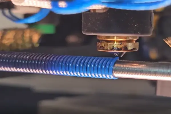
At the heart of this expanded alliance is a dedicated new infrastructure: SIIX has successfully deployed specialized ultrasonic spray coating equipment, establishing a dedicated, state-of-the-art coating environment designed explicitly for prototype trials. By uniting Electroninks’ pioneering metal-organic decomposition (MOD) conductive ink chemistry with SIIX’s massive, globally distributed Electronics Manufacturing Services (EMS) infrastructure, the two companies are providing OEMs with a practical, highly adaptable pathway to transition away from legacy mechanical shielding enclosures toward lightweight, highly conformal, additive solutions.
Executive Overview: Bridging Advanced Materials and Global EMS Scale
The intersection of advanced material science and high-volume electronics manufacturing has historically been plagued by lengthy development cycles and rigid production parameters. The Electroninks-SIIX collaboration is designed to shatter this bottleneck.
Under the terms of the expanded agreement, SIIX will act as an authoritative distribution and collaborative integration partner for Electroninks’ proprietary EMI shielding materials and deposition processes throughout Japan. Rather than pushing customers toward a rigid, pre-determined manufacturing routine, the partnership relies on a hands-on, consultative co-development model.
[ Electroninks MOD Conductive Inks ]
               │
               ▼
[ SIIX Specialized Ultrasonic Spray Setup ]
               │
               ▼
[ Collaborative Prototype Trials (e.g., PBT Plastics) ]
               │
               ▼
[ Production-Ready Conformal EMI Shielding ]
Starting at the prototyping phase, engineers from both organizations work directly with clients to optimize printing and coating dynamics for specific geometries and material sets—including notoriously tricky automotive-grade engineering plastics like Polybutylene Terephthalate (PBT).
This joint initiative directly addresses the compounding pressures faced by hardware developers. As vehicles transition into "data centers on wheels" driven by advanced driver-assistance systems (ADAS), electric vehicle (EV) power control units (PCUs), and complex electronic control units (ECUs), managing internal and external electromagnetic noise is paramount. Traditional stamped metal cans and heavy enclosures add excess weight, complicate assembly flows, and eat up valuable spatial volume. Additive, spray-coated EMI shielding offers a paradigm shift: direct-write, conformal metallic layers deposited precisely where needed on complex three-dimensional geometries, yielding considerable weight savings and unconstrained design flexibility.
Detailed Chronology: The Evolution of Additive EMI Shielding
To understand the weight of this announcement, it is necessary to examine the trajectory of both companies and how their partnership has matured to tackle structural challenges in high-frequency electronics.
Phase 1: Foundational Innovations in Metal Complex Inks
For years, the electronics manufacturing sector relied heavily on particle-based conductive pastes and traditional physical vapor deposition (PVD) methods to apply shielding layers. While functional, these methods presented distinct limitations regarding material waste, geometric versatility, and processing complexity.
Electroninks disrupted this landscape through the commercialization of its proprietary metal-organic decomposition (MOD) inks. Unlike particulate inks that rely on suspended metal flakes, Electroninks’ metal complex formulations—spanning silver, gold, platinum, nickel, and copper—behave as true solutions. Upon thermal processing, these inks decompose to form highly conductive, continuous metallic films. This chemistry enabled direct printing and precision spray-coating on non-traditional substrates, opening the door for additive electronics manufacturing.
Phase 2: Early Collaboration and the EMS Bottleneck
As Electroninks refined its chemical portfolio, scaling these innovations for tier-one manufacturers required deep manufacturing infrastructure. SIIX Corporation, a long-standing partner with deep roots in global Electronics Manufacturing Services (EMS), recognized the potential of MOD technology early on.
However, translating advanced materials from a laboratory bench to high-throughput manufacturing floors requires specialized application environments. Spraying complex metal-organic inks uniformly across multi-planar, three-dimensional electronic housings demands precise control over droplet size, spray velocity, thermal curing profiles, and environmental parameters.
Phase 3: Establishing the Specialized Ultrasonic Spray Environment
The current announcement marks a mature leap forward in this operational relationship. Recognizing the nuanced requirements of additive coatings, SIIX invested heavily in establishing an advanced, specialized ultrasonic spray coating environment.
This installation is not merely a piece of hardware; it is a collaborative proving ground. By integrating precision ultrasonic nozzles—which atomize liquids into highly uniform, micro-sized droplets—SIIX can now execute sophisticated prototype trials for customers across automotive, medical, and industrial sectors. This infrastructure bridges the critical gap between raw chemical formulation and industrial-scale manufacturability, allowing joint customers to validate process parameters before committing to capital-intensive volume production.

Supporting Context & Technical Metrics: Why Additive Shielding Matters
Electromagnetic interference has grown exponentially more complex as consumer and industrial electronics shift toward higher frequency bands, including 5G telecommunications, millimeter-wave radar, and high-frequency switching in electric vehicle powertrains.
The Limitations of Legacy Shielding
- Component-Level Constraints: Traditional stamped metal cans require dedicated mechanical clearance, mounting clips, and manual or automated pick-and-place soldering steps.
- Weight Penalties: Heavy metal enclosures increase total vehicle or device weight, directly undercutting range efficiency in electric vehicles and portability in consumer electronics.
- Geometric Inflexibility: Stamped enclosures cannot easily conform to irregular, organic, or tightly packed housing shapes, leaving vulnerable gaps where electromagnetic leakage can occur.
The Additive Advantage: Precision, Weight, and Performance
Electroninks’ additive EMI shielding platform directly resolves these issues through several key technical mechanisms:
- Conformal Deposition: Precision spray systems apply conductive layers directly to the contours of plastic housings, ECUs, and PCUs. This eliminates the dead space required by physical metal cans.
- Material Versatility: The co-development process is specifically tuned to adhere to ubiquitous automotive and industrial plastics, such as PBT, ensuring robust mechanical bonding without peeling or delamination under thermal stress.
- Optimized Conductivity: Electroninks’ nickel and copper MOD formulations deliver high electrical conductivity at reduced film thicknesses, ensuring exceptional shielding effectiveness (SE) across broad frequency spectrums.
- Supply Chain Agility: By utilizing a scalable EMS framework, manufacturers can iterate designs rapidly during the prototyping phase and seamlessly scale up without changing core material chemistry.
Official Statements: Perspectives from Leadership
Industry leaders from both organizations emphasize that this expanded partnership represents a fundamental shift in how electronic components are conceived and manufactured.
"As electronics across automotive and many other industries become denser and operate at higher frequencies, EMI shielding is evolving from a component-level consideration into a system-level engineering challenge," said Takashi Mochizuki, Director of Sales and Business Development at Electroninks.
"This collaboration brings together advanced conductive materials, a specialized ultrasonic spray coating environment, and global manufacturing expertise so we can work directly with customers to establish coating processes suited to their products, from automotive electronics to a broad range of other applications."
The collaborative ethos is central to the operational framework. Rather than presenting a "black box" solution, Electroninks and SIIX work hand-in-hand with customer engineering teams to fine-tune variables such as wet-film thickness, atomization pressure, and thermal cure cycles for specific product geometries.
"Additive manufacturing is enabling entirely new approaches to electronics integration," added Melbs LeMieux, Co-founder and President at Electroninks.
"By combining advanced materials with scalable EMS manufacturing, SIIX—a longtime partner of Electroninks—is taking strong initiative to advance their EMS business and offer their customers genuine advancements in functionality and production times. We are proud to support SIIX and the overall market in Japan as they look to adopt MOD technology in their electronics manufacturing supply chains."
Future Outlook: Scaling Across Geographies and Markets
Looking ahead, the collaboration between Electroninks and SIIX is structured for continuous evolution. The established technical framework is intentionally modular: as Electroninks introduces new iterations of its conductive metal complex inks—including advanced copper and nickel formulations optimized for cost-effective shielding—both companies can rapidly integrate these materials into existing equipment setups.
While automotive applications—specifically ECUs, power control units, and sensor housings—represent an immediate focal point, the joint venture is positioned to expand into broader semiconductor packaging workflows, consumer electronics, wearable tech, and medical devices.
By de-risking the adoption curve through accessible prototype trials in SIIX’s specialized Japanese coating environment, Electroninks and SIIX are effectively clearing the path for widespread industrial adoption. As high-frequency electronics continue to push physical boundaries, this partnership provides the manufacturing maturity required to keep next-generation systems quiet, lightweight, and exceptionally reliable.
About Electroninks Incorporated
Electroninks Incorporated stands as a global vanguard in the commercialization of advanced materials for electronics and semiconductor packaging. Developing a robust suite of proprietary metal complex conductive ink solutions—including silver, gold, platinum, nickel, and copper—the company accelerates time-to-market for breakthrough innovations and drop-in manufacturing upgrades.
Electroninks’ conductive inks provide high-reliability solutions across printed circuit board (PCB) manufacturing, advanced semiconductor packaging, consumer wearables, medical electronics, and industrial systems. By collaborating closely with elite equipment manufacturers and systems integrators, Electroninks delivers comprehensive material-and-process solutions designed to minimize manufacturing overhead and systemic complexity.
To learn more about Electroninks’ advanced manufacturing solutions, visit www.electroninks.com.