








Executive Overview
For nearly half a century, ultrafast lasers have occupied an exalted status within the pantheon of modern optics. Operating on timescales measured in hundreds of femtoseconds—quadrillionths of a second—these precision instruments have fundamentally reshaped scientific inquiry and high-tech manufacturing. From performing delicate ophthalmic corrective surgeries to anchoring the stability of Nobel Prize-winning optical frequency combs that power the world’s most accurate atomic clocks, ultrafast lasers are indispensable to the architecture of contemporary measurement and engineering.
Yet, despite their transformative capabilities, these systems have historically suffered from a major operational limitation: their physical bulk. Traditional femtosecond lasers are complex, delicate apparatuses that demand expansive optical tables, rigorous environmental stabilization, and considerable financial investment. They are anchored to laboratory basements, manufacturing hubs, and specialized research facilities, largely barred from field deployment due to their size, power requirements, and sensitivity to physical perturbation.
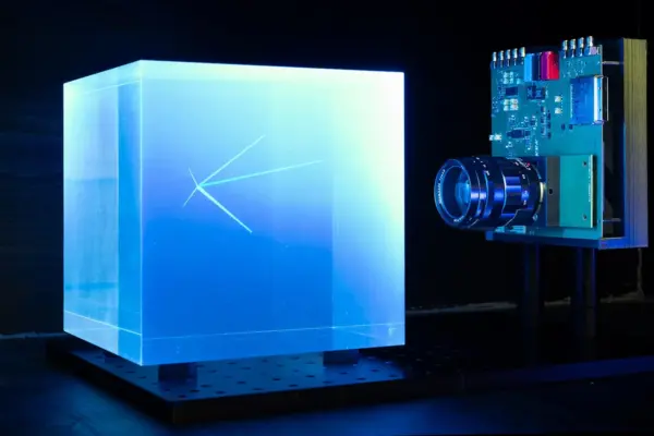
Now, a team of researchers led by Professor Tobias J. Kippenberg at the École Polytechnique Fédérale de Lausanne (EPFL), in collaboration with scientists from the Helmholtz-Zentrum Dresden-Rossendorf (HZDR), has achieved a scientific milestone that shatters this paradigm. Writing in the prestigious journal Nature, the research collective has unveiled the world’s first integrated ultrafast laser capable of matching the raw performance metrics of conventional, room-sized tabletop systems.
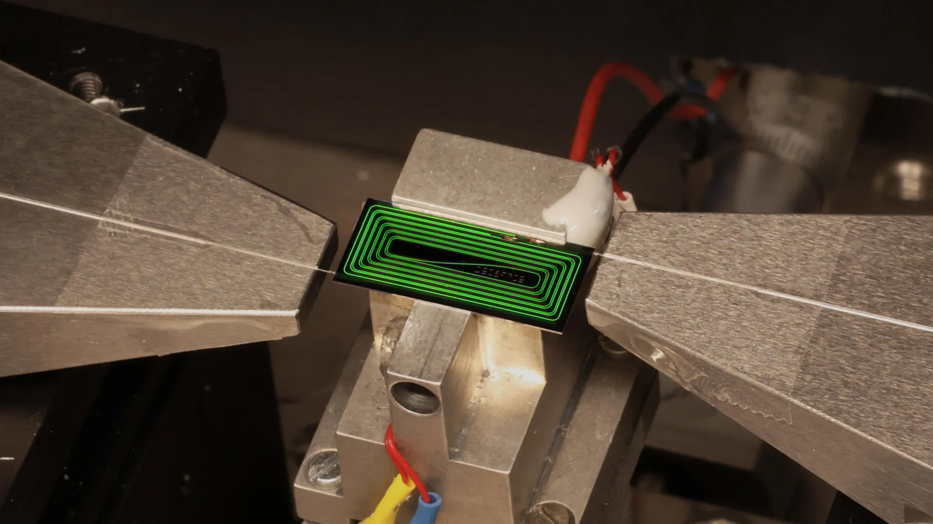
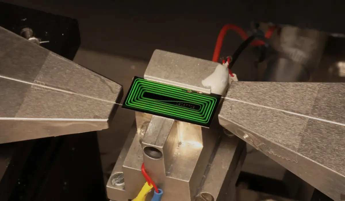
Measuring no larger than a match head yet engineered onto an advanced photonic chip, this breakthrough device delivers pulse energies of 1.05 nanojoules with pulse durations as short as 147 femtoseconds. By successfully translating the power of femtosecond pulses into a scalable, wafer-manufactured semiconductor framework, the EPFL team has realized what the integrated photonics community has long pursued as the ultimate "holy grail" of optical engineering. This development promises to democratize ultrafast optics, transitioning high-power laser technology out of the specialized laboratory and into portable, ubiquitous, and mass-producible formats.
Detailed Chronology: The Road to Integrated Ultrafast Photonics
The Genesis of Ultrafast Optics
The trajectory of ultrafast science began in earnest with the advent of mode-locking techniques in the 1970s and 1980s, which allowed physicists to generate pulses of light lasting mere picoseconds, and eventually femtoseconds. As pulse durations plummeted, peak powers soared into the megawatt and gigawatt regimes, despite average power levels remaining modest. This concentration of energy in microscopic temporal windows unlocked nonlinear optics—phenomena that occur only under extreme electromagnetic field strengths.
Over the subsequent decades, titanium-doped sapphire (Ti:sapphire) lasers and erbium-doped fiber lasers became the gold standard for generating these ultrashort bursts. However, these systems remained bound to macroscopic configurations. Mirrors, lenses, gain media, and saturable absorbers had to be meticulously aligned on heavy optical breadboards to prevent thermal drift and mechanical misalignment.
The Rise of Silicon Photonics
The past twenty years have witnessed a parallel revolution in micro- and nano-electronics: the rise of silicon photonics. Borrowing fabrication techniques from the multi-billion-dollar semiconductor industry, researchers learned to carve microscopic pathways—known as waveguides—into silicon, silicon nitride, and other dielectric substrates. Just as copper wires direct electrical signals on a printed circuit board, these photonic waveguides guide, split, and filter light with extreme precision.
While telecommunications eagerly embraced photonic integrated circuits (PICs) to handle the exponentially growing bandwidth of global data traffic, transitioning high-energy pulsed lasers onto these chips proved exceptionally difficult. The primary obstacle lay in the physics of light confinement. When high-intensity light is squeezed into sub-micron waveguides, power densities skyrocket. This extreme confinement triggers unwanted nonlinear optical effects—such as catastrophic self-phase modulation, stimulated Brillouin scattering, and multiphoton absorption—that typically destroy the laser pulse, warp its spectral characteristics, or physically damage the chip itself.
Overlooking the Obvious: The Mamyshev Oscillator Breakthrough
To solve this long-standing dilemma, the EPFL researchers took a counterintuitive approach. Rather than inventing an entirely new class of nonlinear physics to tame chip-scale light, they resurrected an overlooked laser architecture originally theorized and demonstrated in macroscopic systems decades ago: the Mamyshev oscillator.
Unlike conventional mode-locked lasers that rely on fast saturable absorbers—components that are notoriously difficult to fabricate reliably on silicon nitride platforms—the Mamyshev oscillator utilizes a pair of spectral filters paired with a nonlinear amplification medium.
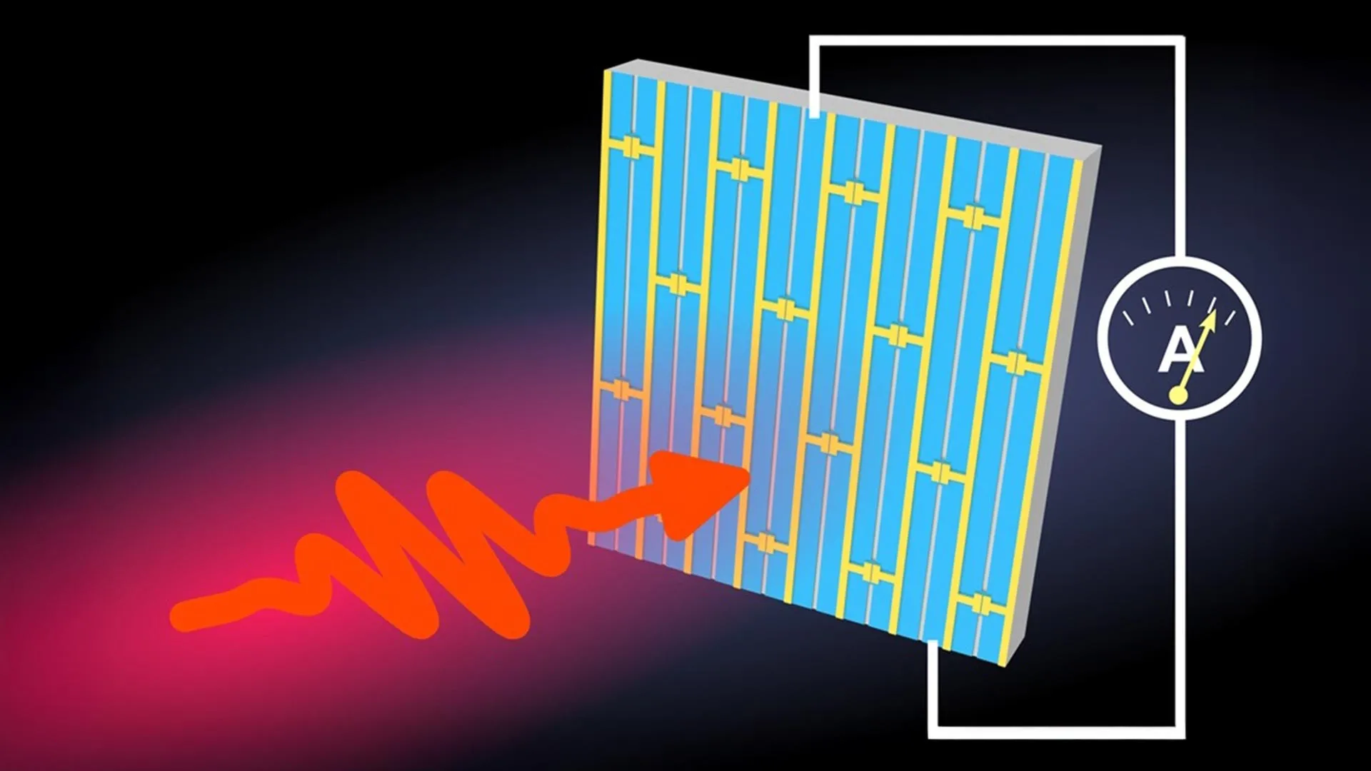
In this architecture, a laser pulse travels through an erbium-doped nonlinear waveguide. As it propagates, the intense pulse undergoes self-phase modulation, broadening its optical spectrum and generating a rich palette of new colors. The pulse then encounters an optical filter that transmits only a specific, shifted portion of this broadened spectrum. Weaker background light or low-intensity noise fails to broaden sufficiently; consequently, it is blocked by the filter and scrubbed from the cavity.
This elegant, self-cleaning mechanism ensures that only robust, high-intensity pulses can successfully circulate within the cavity, stabilizing the laser without requiring delicate, fault-prone physical components. By implementing this design on an erbium-doped silicon nitride photonic platform, the EPFL team bypassed the hurdles that had stalled micro-laser development for a generation.
Supporting Context & Metrics: Decoding the Chip-Scale Powerhouse
To fully grasp the magnitude of the EPFL breakthrough, it is essential to examine the quantitative performance metrics achieved by the chip-scale Mamyshev oscillator alongside the physical realities of its manufacturing process.
Core Performance Metrics
- Pulse Energy: 1.05 nanojoules (nJ). While a nanojoule may sound minute, when compressed into a temporal window of less than 200 femtoseconds, it yields…
- Peak Power: Kilowatt-level peak power. This immense concentration of instantaneous energy is what enables the laser to drive demanding nonlinear interactions required for advanced sensing and metrology.
- Pulse Duration: 147 femtoseconds. Short enough to capture molecular dynamics, chemical reactions, and ultrafast electronic transitions in real time.
- Cavity Footprint: The physical laser cavity spans 42 centimeters in unrolled length, yet through sophisticated optical folding and waveguide routing, it is compacted onto a silicon photonic die no larger than a standard match head.
+-------------------------------------------------------------------+
|                        CHIP-SCALE METRICS                         |
+---------------------------+---------------------------------------+
| Metric                    | Value                                 |
+---------------------------+---------------------------------------+
| Pulse Energy              | 1.05 nJ                               |
| Pulse Duration            | 147 fs                                |
| Peak Power                | Kilowatt-level                        |
| Optical Footprint         | Match-head sized die (~42cm folded)   |
| Manufacturing Yield       | >1,000 cavities per standard wafer    |
+---------------------------+---------------------------------------+
Wafer-Scale Manufacturing Economics
Perhaps the most disruptive aspect of the EPFL research is not merely that the laser works, but how it can be made. Traditional tabletop ultrafast lasers are artisan instruments. They are assembled by skilled optical engineers taking hours or days to align mirrors and cavity lengths with micrometer precision. Each unit is expensive, heavy, and unique.
In stark contrast, the EPFL silicon nitride chips are produced using standard complementary metal-oxide-semiconductor (CMOS) compatible fabrication processes. This means that lithographic masks can pattern thousands of identical laser cavities onto a single semiconductor wafer simultaneously. According to the research team, a single manufacturing run can yield upwards of 1,000 laser cavities on a single wafer substrate.
This transition from handcrafted optical assemblies to semiconductor mass production introduces economies of scale previously unimaginable in ultrafast optics. Just as microprocessors transformed computing from room-sized mainframes into ubiquitous personal devices, wafer-scale photonics promises to slash the unit cost of femtosecond lasers by orders of magnitude, paving the way for widespread commercial adoption.
Official Statements and Expert Perspectives
The breakthrough has generated substantial excitement across the global photonics and physics communities, underscoring both the fundamental elegance of the design and its far-reaching implications.
Reflecting on the historical significance of the achievement, Professor Tobias J. Kippenberg noted:
"For more than twenty years, a high-pulse-energy femtosecond laser on a chip was widely regarded as the holy grail of integrated photonics. Our result shows that it is not only possible, but that it can be achieved with a surprisingly elegant architecture that the integrated-photonics community had largely overlooked."
Addressing the technical challenges overcome during the development phase, co-leading author Zheru Qiu emphasized the compatibility of the Mamyshev architecture with standard manufacturing constraints:
"This design is especially attractive because it does not require any component that is difficult to make on this erbium-doped silicon nitride chip. Photonic chips confine light to extremely small waveguides, causing light to interact strongly with itself. In many laser architectures, these nonlinear effects can destabilize the laser pulses. The Mamyshev oscillator, however, is far less susceptible to these problems, making it particularly well suited for integrated photonic devices."
Highlighting the practical utility of the device in real-world operating environments, Qiu further elaborated on its capability to replace bulky hardware:
"With kilowatt-level peak powers, the chip can drive demanding applications that have long depended on large, expensive laboratory lasers. We are looking at a paradigm shift where field-deployable, high-power ultrafast optics become the standard rather than the exception."
Future Outlook: Transforming Industries from Diagnostics to Navigation
The miniaturization of ultrafast lasers is not merely an incremental engineering upgrade; it is an enabling technology that opens entirely new domains of application previously closed off by the sheer size, fragility, and cost of conventional hardware.
1. Environmental Monitoring and Sensing
High-precision spectroscopy relies heavily on ultrafast laser sources to probe molecular absorption signatures in the atmosphere. With match-head-sized femtosecond lasers, environmental monitoring stations can be deployed across remote ecosystems, mounted on unmanned aerial vehicles (UAVs), or integrated into satellite payloads. These portable sensors will be capable of tracking greenhouse gases, industrial pollutants, and trace chemical signatures with unprecedented spatial and temporal resolution.
2. Non-Destructive Material Testing and Advanced Manufacturing
In industrial settings, ultrafast lasers are prized for "cold ablation"—the ability to machine, cut, or drill materials without transferring thermal energy to the surrounding substrate, preventing micro-cracking and deformation. Chip-scale ultrafast lasers could be embedded directly into automated robotic manufacturing heads, hand-held inspection tools, or quality-control units, allowing real-time, non-destructive testing for structural defects in aerospace components, semiconductors, and medical implants.
3. Next-Generation Medical Diagnostics
Biophotonics stands to benefit immensely from the EPFL breakthrough. Multiphoton microscopy, optical coherence tomography (OCT), and dermatological treatments currently depend on bulky, water-cooled laser systems. Integrating high-energy femtosecond sources onto robust, portable chips could lead to handheld diagnostic scanners that visualize cellular structures deep within human tissue in real time, transforming point-of-care diagnostics and surgical guidance.
4. Compact Optical Atomic Clocks and Navigation
Optical frequency combs—powered by ultrafast lasers—represent the bleeding edge of timekeeping, losing less than a second over billions of years. However, their size has kept them tethered to metrology institutes. Miniaturized ultrafast lasers are a critical stepping stone toward portable optical atomic clocks. These compact timekeeping units will enhance deep-space navigation, synchronize global telecommunication networks, and provide ultra-precise backup positioning systems (GPS-denied navigation) for aviation and maritime operations.
Conclusion
The successful demonstration of a chip-scale Mamyshev oscillator by Professor Kippenberg’s team at EPFL marks the crossing of a major technological Rubicon. By marrying the extreme physics of femtosecond light pulses with the scalable economics of silicon semiconductor manufacturing, the research collective has effectively liberated ultrafast optics from the optical table. As this technology matures and transitions from academic laboratories to commercial foundries, the ripples will be felt across medicine, manufacturing, metrology, and global communications—heralding an era where the immense power of ultrashort light pulses fits comfortably in the palm of a hand.